|
|
|
| RF Front-end |
|
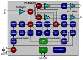
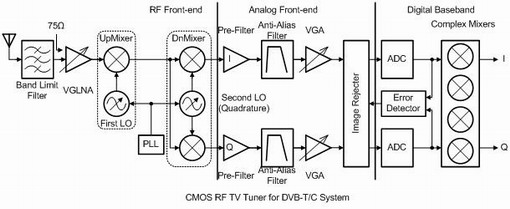
| System Architecture of a DLIF DTV Tuner. |
CMOS RF DTV tuner is a challenging RF front-end circuit, which translates input RF signal with 6/7/8 MHz bandwidth in 50-860MHz into a Low IF at 7.2MHz. To be integrated with digital demodulation circuits, Dual-conversion Low-IF architecture (DLIF) is a better choice, because DLIF architecture avoids DC offset and flick noise in I & Q paths. The final goal of this R&D project is to reduce the requirement of the external components, die size to a small die size about 9mm2, power consumption to about 200mW, and to integrate with other digital circuits in a CMOS process. |
Sponsors:
2004/1-2005/12 : Shanghai STC SDC program (NO. 037062019)
2005/1-2006/12 : Shanghai AM Funds (NO. 0425)
2007/6-2009/5 : National 863 Program (No. 2007AA01Z282)
2009/1-2010/12 : National Science Funding of China (No. 60876019)
|
 |
Wideband variable-gain LNA
A single-ended wideband CMOS LNA with noise-canceling technique ('05-'06)
 |
 |
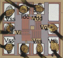
LNA chip. |
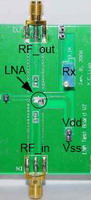
Test PCB. |
A wideband CMOS low-noise amplifier (LNA) is designed in which the thermal noise of the input MOSFET is canceled exploiting a noise-canceling technique. The LNA chip was implemented in a 0.25-µm 1P5M RF CMOS process. Measured results show that in 50-860 MHz, the voltage gain is about 13.4 dB, and the NF is below 3.5 dB with a minimum NF of 2.4 dB at 350 MHz. The input-referred 1dB compression point is -6.7 dBm and the IIP3 is 3.3 dBm. The chip consumes 30 mW at 2.5-V power supply and the chip size (including pads) is only 0.47mm*0.44mm.
A differential variable-gain wideband CMOS LNA ('06)
 |
 |
Differential LNA die (for individual test purpose, without VGA). |
Differential variable-gain LNA for DTV Tuner system. |
A differential variable-gain wideband CMOS LNA for DTV Tuner application (bandwidth 50-860MHz). The proposed circuit uses an off-chip balun as DC feedback, a cross-coupled capacitance transconductance topology and a NMOS load. The simulated gain variable from -10~14dB by 3dB step, S11 below -20dB, NF below 4dB, IIP3 great than 8dBm, with 5.8mW power dissipation. The chip is designed with a 0.18μm CMOS process |
|
|
Up and down conversion mixers
Wideband upconversion mixer
 |
| Wideband upconversion mixer. |
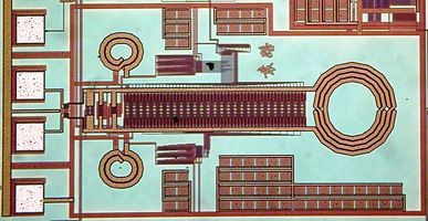
The upconversion mixer converts the input RF signal to a high first IF at 1120MHz. So the input signal is broad band while the output is narrow band. The relative tuning range of LO is much reduced with high sideband mixing. Compared with the traditional
Gilbert architecture, the transconductors are modified with multi-tanh principle to achieve better linearity. LC tank is employed as load impedance due to its frequency selection characteristic and other advantages. The main specification is as follows: Conversion Gain>5dB; Noise Figure<10dB; IIP3 >10dBm.
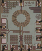
Image-rejection quadrature downconversion mixer
 |
| Image-rejection quadrature downconversion mixer. |
The quadrature downconversion mixer transfers the 1120MHz RF signal with 6-8MHz bandwidth to 7.2MHz Intermediate Frequency. The quadrature conversion adopts the topology with shared transconductor stag between I/Q paths, which proves to achieve improved CG, NF and power consumption compared with conventional mixer pair in commutating mode. This topology also relax the design trade-off between transconductor stage and switching stage, as the bias current in the transconductor stage is halved between I and Q path. In addition, the linearity of mixer is improved through the adoption of Multiple-Gated Transistor in transconductor stage. Special layout technologies, such as common-centroid, inter-digitation, dummy, symmetry etc., are utilized to attain good matching and high IIP2. Fabricated in a 0.18-μm 1P6M RF CMOS Process and consumes only 3mA current from 1.8-V power supply, the quadrature mixer measures a conversion gain of 12.5dB, an IIP3 of 10dBm, an IIP2 of 58dBm, and an SSB noise figure of 17.6dB, which indicates its feasibility in low cost zero-IF or low-IF applications.
|
|
|
High performance LC VCOs
Wideband LC VCO
 |
| Wideband LC VCO. |
A wideband LC voltage-controlled oscillator (VCO) is used in DTV tuner systems, which is implemented in a 0.18μm CMOS process. A switched varactor array is proposed to suppress tuning gain fluctuation for the performance of the phase locked loop (PLL). Measured results show that the tuning range achieves 860MHz from 1.17 to 2.03 GHz with the tuning gain from 69 to 93 MHz/V. The measured phase noise is -126dBc/Hz at 1MHz offset frequency. Power consumption is about 9 mW at a 1.5 V supply voltage.
Transformer-based quadrature LC VCO
 |
| Transformered-base quadrature LC VCO. |
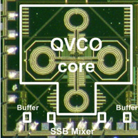
A transformer-based quadrature multi-band LC-VCO (QVCO) with differentially tuning is implemented in 0.18-μm CMOS. At 1.5V supply voltage and a core power dissipation of 6mW, the QVCO realizes a tuning rage from 980 MHz to 1.195 GHz with the measured phase noise of -131dBc/Hz at 1 MHz offset. The measured worst case of image rejection ratio (IBR) is 47dB across the whole tuning range, which corresponds to a quadrature phase error of 0.5°.
|
|
|
Frequency synthesizers
Wideband integer-N frequency synthesizer
 |
| 1.175 to 2GHz frequency synthesizer. |
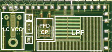
A fully integrated 1.175 to 2GHz differentially tuned frequency synthesizer aimed for DTV tuners is implemented in 0.18-μm CMOS. It exhibits in-band phase noise of -97.6dBc/Hz at 10kHz offset and integrated phase error of 0.63° from 100Hz to 10MHz. Variations of VCO tuning gain are compensated for maintaining loop stability and phase noise optimization. The AFC (Automatic frequency control) locking time is only 16μs with 4bits control. The chip draws 18mW from a 1.8V supply while occupying 2.6mm2 die area.
Narrowband sigma-delta fractional-N frequency synthesizer
 |
| 1.1GHz sigma-delta fractional-N frequency synthesizer. |
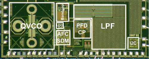
A fully integrated 1 to 1.175GHz differentially tuned sigma-delta fractional-N frequency synthesizer aimed for DTV tuners is implemented in 0.18-μm CMOS. It exhibits in-band phase noise of -95dBc/Hz and -130dBc/Hz at 1MHz offset in integer-N mode, while -80dBc/Hz and -120dBc/Hz in fractional-N mode. The AFC (Automatic frequency control) locking time is only 21μs with 5bits control and the frequency resolution is 12Hz. The chip draws 18mW from a 1.8V supply while occupying 4.42mm2 die area.
High-performance fully-differential charge pump
 |
| Fully-differential charge pump. |
A PLL based on a charge pump is preferred over other types because it has a wide capture range and no systematic phase offset.In high-performance applications with stringent noise suppression requirements, a fully differential charge pump is preferred over a single-ended charge pump because of the immunity to common-mode noise and power supply variation. We try to propose a fully differential charge pump circuit, which has a stable CMFB circuit, high-speed response, perfect current mismatch suppression and low in-band noise in fractional-N PLLs.
|
|
| Analog IC Design |
Analog-to-digital converter(ADC), Digital-to-analog converter(DAC), Viaralbe gain amplifiers(VGA), Anti-alias filter, Bandgap & LDO |
|
Analog-to-digital converter(ADC)
 |
| 3.3V 10-bit 100MHz pipelined ADC. |
This chip was manufactured in Chartered 0.35μm double-poly four-metal CMOS mixed-signal process. The die area is 1.2×1.1mm2. The power dissipation is 142mW with 3.3v power supply. SNDR is 58.7dB when sampling 42MHz sinusoid input signal at 100MHz sampling clock.
|
|
|
Digital-to-analog converter(DAC)
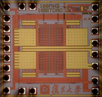 |
| 10-bit 100MHz current-steering DAC. |
A 10-bit 100MSample/s current-steering CMOS digital-to-analog (D/A) converter is presented. A “6+2+2” segmented architecture is adopted. The six most significant bits and the intermediate two bits are thermometer encoded and steer a unary current source array, while the two least significant bits are binary weighted. The unary current cell and the generated circuit of switching control signals are carefully optimized in order to minimize the glitch energy. The chip has been implemented in TSMC (1P5M) 0.25-μm CMOS technology and has an active area of 910μm×970μm. The measured differential nonlinearity (DNL) and integral nonlinearity (INL) are within ±0.6LSB and ±1.2LSB respectively. The maximum output glitch energy is 0.436pV s. The power consumption is 86.2mW, and it operates at a 3.3V analog voltage supply and a 2.5V digital voltage supply.
|
|
|
Anti-alias filter
 |
| Anti-alias Opamp-RC filter. |
The main purpose of the analog baseband filter is to select the desired channel and maximize the dynamic range of ADC. In CMOS technology, Active RC, MOSFET-C and Gm-C filters are the most popular baseband filters. Here, we designed a 12-order butterworth Active RC filter to achieve good dynamic range, frequency attenuation and low distortion. The time constant of integrated filter determined by R and C, and may vary ±50% with the variation of process and temperature, so, the tuning circuit was designed to meet frequency precision 5%.
|
|
|
Bandgap and low drop-out regulator
 |
 |
Low noise bandgap. |
Low dropout regulator. |
Bandgap circuit provides a DC voltage which is independent of the supply and process, and then, we can get a stable current bias for the whole chip through V-to-I circuit. We also need the Bandgap voltage connect with LDO to supply the VCO, so, low noise output and high PSRR of LDO is essensial to assure the phase noise of VCO. Here, we design a low noise Bandgap and LDO to meet the requirement. The total integrated noise from 1Hz to 100KHz is 11uvrms, the PSR achieves -66.5dB@DC, and -40dB@1MHz.
|
|
| Device Modeling |
The device modeling research provides better modules performance and more choices for both circuit topologies and device parameters. The currently research on device modeling focus on mainly three areas, which are on-chip inductors, on-chip multi-layer MIM capacitors, and CMOS compatible BJTs. |
|
On chip inductors
Differentially driven inductors
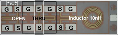 |
| Differentially driven inductors. |
It shows the microphotograph of an on-chip multilayer inductor, which includes an open and thru de-embedding structure to cancel the parallel capacitors in the bondpads and the in-series resistors of Al-interconnection. The differentially driven 10nH inductor uses multilayer Al metals, M5 in series with the paralleled M4//M3//M2, and only occupies 250μm by 250μm with a trace width of 15μm and spacing of 2μm. It measures a differential inductance about 9.44nH, and a differential Q about 6 at 1.0GHz.
Center-tapped differential inductors
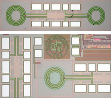 |
| Center-tapped differential inductors. |
A center-tapped equivalent model of the center-tapped differential inductors is proposed. The single-ended and differential impedances in differential applications are derived respectively. A 2-port S-parameter measurement with the center-tap grounded is used to extract the equivalent resistance, inductance and Q-factor (RLQ). A multi-layer center-tapped differential inductor is implemented in a 0.35 μm 1P4M RF CMOS process. The proposed model agrees well with the experimental results below the self-resonance frequency.
|
|
|
|